
What you are about to read is a handout and certainly not a book and therefore does not claim to be exhaustive and self-sufficient. This can be accompanied by documentation that can be easily found both in paper and digital form. For the drafting of this handout, in addition to the obvious information that can be found online, I took extensive inspiration from the Z80 Programming in Assembly language manuals and the New Z80 manual. As with all my other articles I apologize for any inaccuracies. Enjoy the reading.
THE CPU AND ITS CONNECTIONS
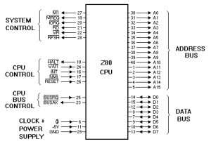
In this article we will describe the various signals that the Z80 CPU presents on its pins. When we talk about input/output we mean it relative to the CPU. What we see below is the functional arrangement of the signals and not their real position in the package.
BUS
In the CPU there are two types of BUS, one called ADDRESS BUS and the other called DATA BUS, let's see what it is.
ADDRESS BUS
This type of bus is called tri-state because it has the ability to virtually disconnect the CPU from the external address bus by placing these output signals in a high impedance state. The outputs are active high and unidirectional (so it is the CPU that generates the addresses). Signals A0-A15 make up the address bus where A0 is the least significant bit. The bus provides addresses for exchanging data with memory and I/O devices. I/O device addressing is done using the least significant 8 bits of the address bus, A0 through A7.
DATA BUS
This type of bus is called tri-state because it has the ability to virtually disconnect the CPU from the external address bus by placing these output signals in a high impedance state. The outputs are active high and bidirectional. Signals D0-D7 constitute the data bus where D0 is the least significant bit. The bus is used to exchange data with memory and I/O devices.
CONTROL SIGNALS
Some texts report in addition to the DATA BUS and ADDRESS BUS also the SYSTEM CONTROL BUS, the latter collects those signals that allow the reading and writing operations to be managed. Having clarified that it is possible to find a different grouping of CPU signals, let's describe the signals that the Z80 makes available to us.
M1 (Machine cycle) – Output active low, indicates that the code of the next instruction is loaded in the current machine cycle (instruction fetch). There are some instructions, having the opcode consisting of two bytes which therefore require two consecutive M1 cycles.
MREQ (Memory Request) – Active low tri-state output, indicates that there is a valid address on the address bus for a read/write operation.
IORQ (Input Output Request) – Active low tri-state output, indicates that there is a valid address for I/O operations on the 8 least significant bits of the address bus. The IORQ signal is also generated together with the M1 signal during the interrupt recognition cycle.
RD (Read) – Tri-state output active low, indicates that the CPU wants to read from memory or an I/O device.
WR (Write) – Tri-state output active low, indicates that the BUS contains valid data to be written to memory or an I/O device.
RFSH (Refresh) – Low active output, used for dynamic memories. Indicates that there is a valid address for refresh on the least significant bits of the address bus.
HALT – Output, active low. Indicates that the CPU has executed a HALT instruction and is waiting for a non-maskable or maskable interrupt signal (if the latter has been previously enabled) to be able to resume program execution. As long as the halt state persists, the CPU continuously executes NOP (No Operation) instructions to maintain the refresh activity as the continuation of this state could lead to the loss of the data contained in the dynamic memories.
WAIT – Input, active low. WAIT tells the CPU that the memory or I/O device is not ready for a data transfer. As long as this signal is active the CPU remains in a waiting state. This signal allows I/O or memory devices of any speed to synchronize with the CPU speed and remains active as long as the unavailability situation persists.
INT (Abort Request) – Input, active low. The interrupt request signal is generated by the I/O devices. The request is satisfied at the end of the instruction in progress, when the executing program foresees it, under the two conditions: – the internal interrupt enabling flip-flop (IFF) controlled by the software is enabled: – The BUSRQ signal is not is active. When the CPU accepts the interrupt, an interrupt acknowledge signal (IORQ at the same time as M1) is sent at the beginning of the next interrupt read cycle. The CPU can respond to the interrupt in three different ways: mode 0, 1, 2.
NMI (Non-Maskable Interruption) – Input, active on the falling edge. The non-maskable interrupt request line has higher priority than the INT line and is active at the end of the current instruction, regardless of the state of the interrupt enable flip flop.
RESET - Entrance. Initializes the CPU: resets the PC, I and R registers. Arranges interrupt management in 0 mode.
BUSRQ (Bus Request) – Input, active low. The signal is used to request the CPU to place the address bus, data bus, and output control signals in the high impedance state, so that these lines can be controlled by the requesting device. When BUSRQ is activated, the CPU places the bus in the high impedance state at the end of the current machine cycle.
BUSAK (Bus Awareness) – Output, active low. This signal is used to indicate to the requesting device that the address bus, data bus, and tri-state control signals of the CPU buses have been placed in the high impedance state and that the external device can control these lines.
CLOCK – Single phase input.
If you are interested you can find it here fourth dispensation.