
What you are about to read is a handout and certainly not a book and therefore does not claim to be exhaustive and self-sufficient. This can be accompanied by documentation that can be easily found both in paper and digital form. For the drafting of this handout, in addition to the obvious information that can be found online, I took extensive inspiration from the Z80 Programming in Assembly language manuals and the New Z80 manual. As with all my other articles I apologize for any inaccuracies. Enjoy the reading.
CPU TIMING
During the design of the Z80 CPU a series of elementary timing cycles were defined, these rigorously dictate all the operations that are carried out to carry out a certain job. Below I will list and then describe these cycles.
- Reading / Writing on memory
- Read / Write on I/O
- Interrupt recognition cycle
Each instruction consists of a sequence of these elementary operations, each of which is executed in a number of clock cycles varying from 3 to 6. The clock period is called cycle T, while each elementary operation is executed in one machine cycle M .
Let's take a look at the most important timing diagrams:
OPERATIONAL CODE LOADING CYCLE (FETCH)
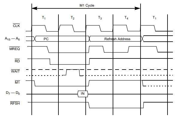
This is the fundamental loop, it is executed on every instruction and is referred to as M1. The Fetch cycle is divided into four clock periods. During the T1 period the contents of the Program Counter (PC) are placed on the address bus and the M1 signal (active low) is activated. Subsequently, in the middle of the period, the MREQ and RD signals are activated (always at low level) in sequence. During the periods T1 and T2 the M1 signal remains active to indicate that in this cycle the code of an instruction is read from the memory. During the T3 and T4 period the CPU decodes the instruction, while the refresh address is available on the address bus.
READING OR WRITING CYCLE IN MEMORY
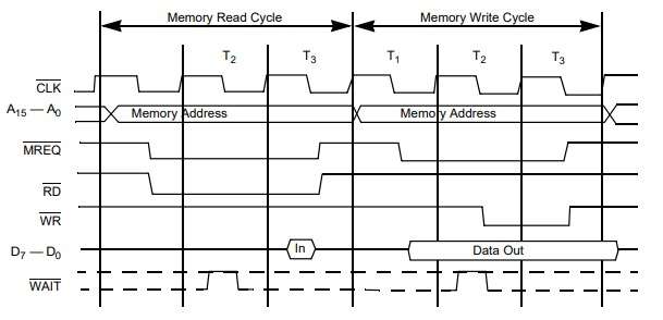
As we can see, the fundamental cycle for reading or writing on a memory is composed of three periods each. The read cycle is similar to the Fetch cycle, as we can see in the T1 period we have a stable address on the address bus, then after half the clock cycle the MREQ and RD signals are activated (active low). As with the Fetch cycle, also in this case it is possible to insert WAIT cycles. In period T3, data is sampled from the data bus on the falling edge of the clock. Subsequently the MERQ and RD signals are deactivated.
For the memory write cycle in period T1 we have a valid address on the address bus. Halfway through the period the MREQ signal will be activated. Towards the end of T1 we have a valid data on the data bus. In period T2, the WR signal is activated on the falling edge of the clock (here we are sure that the data is stable). The data will remain present on the data bus for the entire period T3 and T4. The WR signal will instead be disabled in the middle of the T3 period.
PERIPHERAL INPUT OUTPUT CYCLE
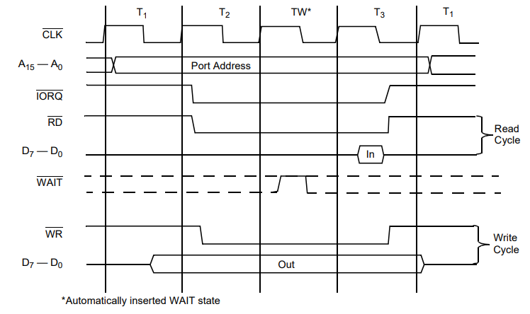
The two basic cycles for reading and writing are illustrated in the figure. During a read operation, the address on the address bus is stabilized in period T1. The IORQ and RD (active low) signals are activated on the rising edge of T2 and remain active until the falling edge of T3. The data presented by the peripheral on the data bus is sampled on the falling edge of T3, as was done in the memory reading cycle.
During the writing cycle, the IORQ and WR signals which indicate a writing operation towards the peripheral are active for the period T2 and T3 as for the reading operation. The data presented by the CPU to the peripheral will be available for as long as the IORQ and WR signals are active. It is notable that the CPU inserts a TW waiting period, so that the entire operation lasts four clock cycles.
INTERRUPT ACCEPTANCE CYCLE
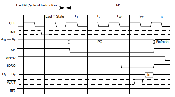
The acknowledgment of an interrupt request occurs during the last period T of each instruction. With the rising edge of the clock we verify that the INT signal is active (low level) and that the BUSRQ and NMI signals are not active (always active low), which have a higher priority than the INT signal. If all conditions are satisfied the next cycle is defined as the interrupt accept cycle. This cycle consists of an M1 cycle where instead of the MERQ signal being active, the IORQ signal is activated. This particular situation is recognized by the peripheral which presents a word (interrupt vector) on the data bus which allows a vectorized response to the interrupt to be created. This is sampled on the rising edge of T3. The WAIT signal is sampled on the falling edge of the second TW, this allows the CPU to insert further wait states if necessary.
NMI AND BUSRQ ACCEPTANCE CYCLE
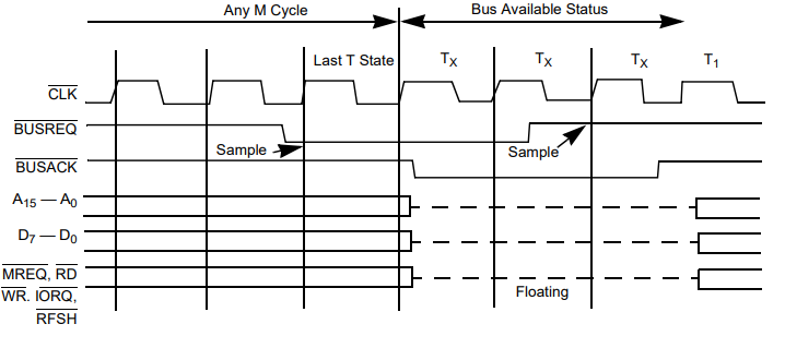
The Z80 is able to recognize NMI and BUSRQ signals as external requests in addition to the normal INT request. The BUSRQ (active low) signal is sampled during the last phase of each machine cycle. If this is active, the CPU puts the address bus, data bus and control signals into a high impedance state. In this state the CPU will not be able to recognize other requests and will simply sample the BUSRQ signal on each rising edge of the clock to return to its normal activity when it returns high.
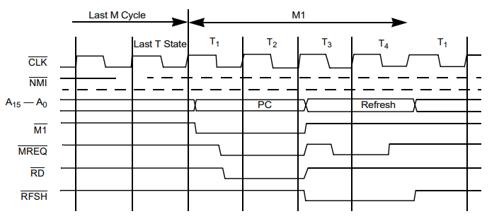
The NMI signal (active low) is sampled during the last cycle of each instruction with the rising edge of the last T cycle, if this is active and BUSRQ is not active, the next M1 cycle is ignored by the CPU and is subsequently accepted the service request as already described for INT.
This handout concludes our introduction to the Z80 CPU. I hope that these provide inspiration for further insights on both the hardware and software side.